Today, I focused on selecting a suitable low noise amplifier (LNA) for operation around 161 MHz, with the goal of building the receiver front end for our RF project. I started by exploring products from two major RF manufacturers: Mini-Circuits and Qorvo. My main criteria were low noise figure, sufficient gain at ~161 MHz, good impedance matching, and practical integration features like shutdown capability and reasonable power consumption. After shortlisting candidates, I carefully reviewed the datasheets of three promising parts: the Mini-Circuits TSS-23ULN+, and Qorvo’s QPL9547 and TQP3M9035.
The Mini-circuits TSS-23ULN+ covers a wide frequency range from 10 MHz to 2 GHz, making it naturally suitable for VHF. From the datasheet, it provides very low noise figure, around 0.3–0.4 dB in the 100–500 MHz range, which is excellent for weak-signal reception. The typical gain is about 24.7 dB at 500 MHz, and slightly higher below that, likely giving us ~26–28 dB at 161 MHz. Input and output return loss are also solid, typically over 13–14 dB, helping with impedance matching. The output power at 1 dB compression (P1dB) is around +20.4 dBm, and the OIP3 (third-order intercept) is high, around +36–37 dBm, ensuring decent linearity. The part operates from a single +5 V supply and uses around 70 mA, and it has a very fast shutdown feature (~7.5 ns), useful for power saving or TDD systems. Overall, this part stands out for its ultra-low noise and balanced performance at our target frequency.
The Quorvo QPL9547 is a broadband LNA covering 0.1–6 GHz, originally optimized for higher bands like 1.9 GHz, but usable at VHF too. Its datasheet shows an excellent noise figure of around 0.3 dB at 1.9 GHz, and this remains low down to ~100 MHz. The typical gain at 1.9 GHz is ~19.5 dB, but at lower frequencies, the amplifier performs better, likely giving us ~23–24 dB gain at 161 MHz. Input and output return loss are reasonable, around 12–14 dB. It offers very strong linearity, with an OIP3 of +39.3 dBm and P1dB around +22–22.8 dBm, which is higher than the Mini-Circuits part. It supports supply voltages from +3.3 V to +5 V and draws about 65 mA, slightly more power efficient than the TSS-23ULN+. A built-in shutdown pin provides quick switching (~80 ns). This part is attractive when linearity is especially important, though it was originally optimized for higher frequencies
Finally, the Quorvo TQP3M9035 is another broadband LNA designed to cover 50–6000 MHz, including low-IF and VHF. In its datasheet low-frequency reference design, it shows very high gain, around 27–28 dB at ~150–200 MHz, which is the highest among the three. Its noise figure is a bit higher, around 0.6 dB, still quite low but not as exceptional as the others. Input and output return loss are good, around 15 dB. It offers strong linearity too, with OIP3 between +38–40 dBm and P1dB around +23 dBm. This part requires higher current, about 115 mA, and works at +5 V. It also has a shutdown control pin. This amplifier is most attractive if maximizing gain is critical and higher current consumption is acceptable.
| Parameter | Mini-Circuits TSS-23ULN+ | Qorvo QPL9547 | Qorvo TQP3M9035 |
| Gain | ~26–28 dB | ~23–24 dB | ~28 dB |
| Noise Figure | ~0.3–0.4 dB | ~0.3 dB | ~0.6 dB |
| P1dB | +20.4–21 dBm | +22–22.8 dBm | +23 dBm |
| OIP3 | ~36–37 dBm | +39.3 dBm | ~38–40 dBm |
| Input Return Loss | ~8–10 dB | ~9–12 dB | ~12 dB |
| Typical Current | ~70 mA | ~65 mA | ~115 mA |
| ShutDown | Yes, 7.5 ns | Yes, 80 ns | Yes |
Table. 1 : Summary Table at 161 MHz
In summary, the TSS-23ULN+ stands out for its very low noise and balanced power, good impedance matching to 50 Ω systems, making it excellent for sensitive receivers. The QPL9547 offers slightly lower gain but higher linearity and power efficiency, and the TQP3M9035 provides the strongest gain and linearity, though it draws more current. For our 161 MHz design, the TSS-23ULN+ remains the most balanced choice. It operates from a single +5 V supply and includes a fast shutdown feature, making it practical for power-sensitive designs.
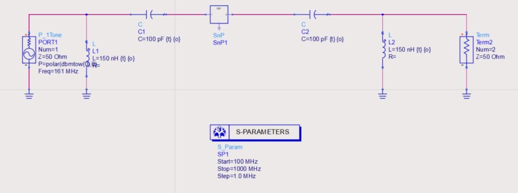
Fig. 1: Schematic of Impedance Matching of TSS-23ULN+
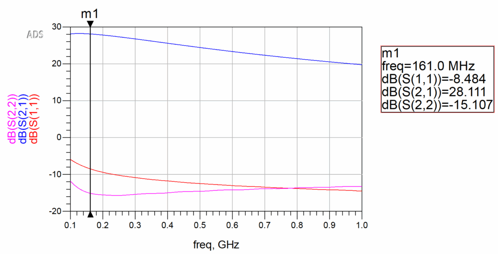
Fig. 2: S-Parameter Simulation of TSS-23ULN+
After choosing the TSS-23ULN+, I downloaded its S2P file and imported it into Keysight ADS to simulate its real S-parameter performance around 161 MHz. I built a matching network in ADS as shown in the schematic, using series capacitors (100 pF) and shunt inductors (150 nH) to tune the input and output impedance. The S-parameter simulation showed promising results at 161 MHz: about +28.1 dB gain (S21), input return loss ~–8.5 dB (S11), and output return loss ~–15 dB (S22). These values confirm the LNA will work well in our band, though the input return loss can be improved.
Looking ahead, my plan is to optimize these passive components further to improve matching, especially to get better S11 closer to –10 dB or better. Once optimized, I plan to replace the ideal lumped components with actual Murata SMD parts (from their libraries) to see realistic parasitic effects and verify performance. This will give a more accurate prediction of the final board’s behavior.
Overall, today’s work underlined the importance of carefully matching component specs to the actual operating frequency. Simulations based on real S-parameter data proved to be an invaluable step in confirming the suitability of the chosen LNA before moving forward to hardware design. Today’s work helped confirm that the TSS-23ULN+ is a strong candidate for our 161 MHz design, and the ADS simulation gave me a clear path forward to fine-tune the matching network before moving to PCB design.
Leave a Reply