Over the past few days, I have been working on the design and simulation of a power amplifier using the AFT05MS004N LDMOS transistor. My objective was to achieve a performance level at 161 MHz that closely aligns with the values specified in the official datasheet of the transistor. I carried out this work using the ADS 2023 environment, utilizing the nonlinear model of the transistor along with harmonic balance simulations.
Initially, I conducted a load-pull analysis to extract the optimal source and load impedances for maximum output power and efficiency. However, the impedance values I used at first were incorrect due to misinterpretation of the impedance contours. As a result, the amplifier performance was significantly off there were deviations in gain, output power, and efficiency when compared to the datasheet specifications. Realizing the importance of accurate impedance matching, I revisited the load-pull process and carefully extracted the correct values.The updated impedance values I obtained were Zs = 7.320 + j11.233 Ω for the source and Zl = 3.920 – j3.010 Ω for the load.
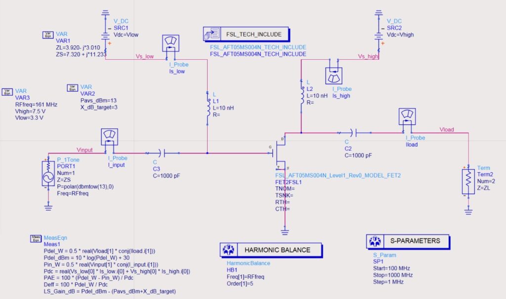
Fig.1: Schematic of Validation of Source and Load Impedance
These were implemented into the schematic using appropriate matching networks, with 1000 pF DC blocking capacitors and 10 nH RF chokes for biasing. Once the matching network was updated, I re-ran the harmonic balance simulation and observed a significant improvement in all key output parameters.
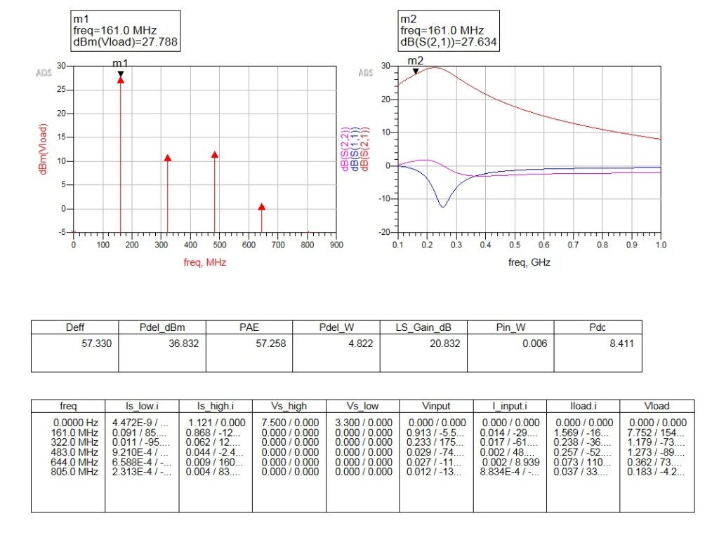
Fig. 2: Simulation of Validation of Source and Load Impedance
The new simulation results at 161 MHz showed an output power of 36.83 dBm, which corresponds to approximately 4.8 W. The gain was measured at 20.83 dB and the power added efficiency was 57.26%. The total DC power consumption was calculated to be 8.41 W. These results were then compared to the datasheet specifications of the AFT05MS004N transistor, particularly at 155 MHz, which is within the same VHF band.
Here is a comparison between the simulated and datasheet values:
| Parameter | Datasheet (155 MHz) | Simulation (161 MHz) |
| Frequency | 155 MHz | 161 MHz |
| Output Power(Pdel) | 6.0 W | 36.83 dBm (~4.8 W) |
| Input Power | 0.06 W | 13 dBm (0.02 )W |
| Drain Efficiency | 69.1 % | 57.26 % |
| Power Added Efficiency (PAE) | Not Specified | 57.26 % |
| DC Power (PDC) | Not Specified | 8.41 |
| Gain | 20.1 dB | 20.83 dB |
| VDS | 7.5 V | 7.5 V |
While the efficiency is slightly lower in the simulation, the output power and gain closely align with the expected values. The differences can be attributed to the frequency shift, component implementation variations, and model limitations. Overall, the match between the simulated and datasheet data confirms the success of the design approach.
Additionally, I evaluated the spectrum and S-parameter response. The fundamental tone in the Vload spectrum appeared clean and strong at 27.8 dBm, confirming minimal harmonic content. The S21 gain at 161 MHz was about 27.6 dB in small-signal conditions, supporting the high gain observed in large-signal simulation.
This project emphasized the importance of accurate load-pull analysis in RF design. After correcting the impedance values, the amplifier performance began to match the manufacturer’s datasheet. I am continuously testing new values and refining the schematic to approach the ideal design. This process has helped me gain hands-on experience with nonlinear transistor modeling, harmonic balance simulation, and RF power amplifier theory and loadpull analysis.
With the successfully validation of source and load impedance and the amplifier parameters now closely matching the datasheet, the next step in my design journey will focus on impedance matching on both the input and output sides. Accurate matching is essential not only for maximizing power transfer but also for ensuring amplifier stability and bandwidth performance. I will be designing matching networks that transform the 50-ohm system impedance to the optimal ZS and ZL extracted from the load-pull results. This stage will include Smith Chart analysis, microstrip line design, and further simulation to ensure minimal reflection and maximum efficiency across the desired frequency range.
Leave a Reply