Today, I continued refining the load-pull simulation of my RF power amplifier based on the AFT05MS004N transistor using ADS 2023. I configured a 1-Tone Load Pull setup targeting a center frequency of 161 MHz, with a gate bias of 3.25 V and a drain bias of 7.5 V, and set the input power level to 25 dBm. The simulation aimed to evaluate both delivered power and PAE (Power Added Efficiency) contours across a sweep of complex load impedances. The setup included sweeping the fundamental load around a center of 20 + j0 Ω using a dense grid of 144 points.
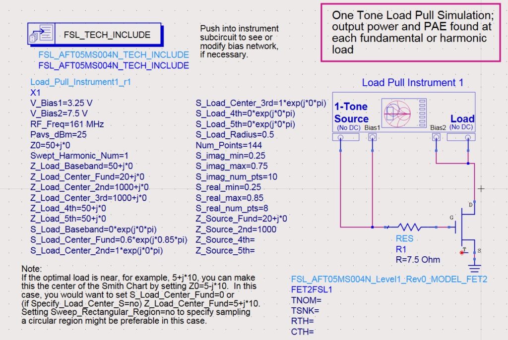
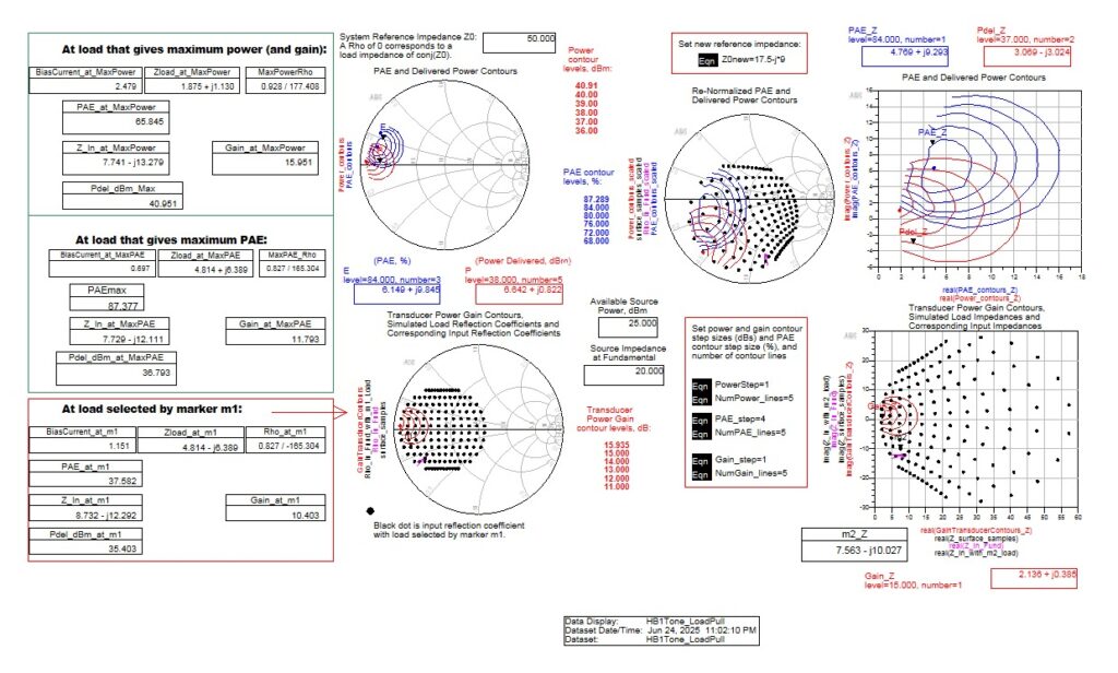
Fig.1 : Schematic and Simulation of Loadpull Analysis at 161MHz
| Parameter | At Max Output Power | At Max PAE |
| Zload (Ω) | 1.875 + j1.18 | 4.814 + j6.389 |
| Pdel (dBm) | 40.951 | 36.793 |
| PAE (%) | 85.845 | 87.377 |
| Gain (dB) | 15.951 | 11.793 |
| Zin (Ω) | 7.741 – j13.979 | 7.722 – j12.111 |
| Bias Current (A) | 2.479 | 0.697 |
After completing the load-pull simulation, I was able to extract two key sets of impedance values—one corresponding to maximum output power and the other to maximum power-added efficiency (PAE). The optimal load impedance for achieving the highest output power turned out to be 1.875 + j1.18 Ω, which allowed the amplifier to deliver 40.95 dBm, or roughly 12.4 watts, of RF power. This setup achieved a gain of 15.95 dB and a PAE of 85.84%, which is quite efficient.
On the other hand, when the goal was maximum efficiency, the best-performing load impedance was 4.814 + j6.389 Ω. While the output power at this point dropped slightly to 36.79 dBm, the PAE improved to an impressive 87.38%, with a gain of 11.79 dB. These results highlight the typical trade-off in RF amplifier design—balancing between raw power output and overall efficiency, depending on the application requirements.
Along with the load impedances, I also captured the corresponding input impedance, which was approximately 7.7 – j13.9 Ω under these operating conditions. This value is critical for designing an effective input matching network that can ensure maximum power transfer from a standard 50 Ω source. I also observed that the bias current varied significantly between the two cases: it was about 2.479 A at maximum output power and dropped to 0.697 A at maximum efficiency.
This variation is important when considering the amplifier’s thermal performance and power supply design. These insights will directly guide how I approach the matching network. If the primary goal is higher RF power say, for longer-range communication I’ll tune the output network to match the maximum power impedance. If efficiency and thermal performance take precedence, then I’ll target the impedance that yields the highest PAE. These decisions are essential as I move into the next design phase.
With these target Zload and Zsource values established, I began working on the impedance matching stage. I created a schematic in ADS 2023, aiming to transform the standard 50 Ω system impedance to the required complex values at 161 MHz. However, once I ran the simulation, I noticed that the results weren’t matching my expectations. Key parameters like return loss, VSWR, and the final impedance at the transistor ports didn’t align with the calculated target values. This indicates that the matching network needs more refinement and that I may need a deeper understanding of how components and transmission lines behave at this frequency.
To move forward, I plan to dig deeper into impedance matching theory. I’ll revisit Smith Chart-based synthesis techniques, analyze different network topologies, and examine how transmission line lengths and component Q-factors affect performance. I also intend to study the frequency response of the current design more carefully to identify the source of mismatches. This next round of detailed analysis should help me adjust the network so it achieves the correct impedance transformation and performs optimally in the overall amplifier circuit.
Leave a Reply