Today, I started by watching an excellent lecture on FET Loadline and Power Amplifier Design by Anurag Bhargava. The video laid out the entire flow of LDMOS amplifier design in ADS, from basic DC-IV simulations to loadline analysis and Class AB biasing. It gave me a clear sense of direction, so I began with the most fundamental step -the DC-IV simulation.
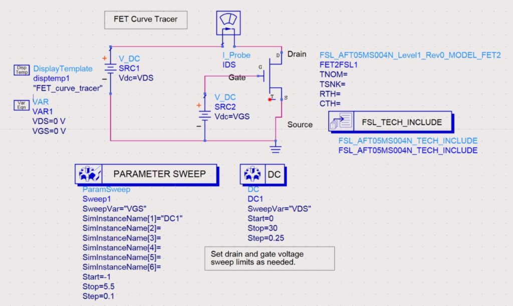
I used ADS 2023 to simulate the AFT05MS004N transistor using a typical curve tracer setup. The drain voltage (VDS) was swept from 0 to 30 V in 0.25 V steps, while the gate voltage (VGS) ranged from -1 to 5.5 V in 0.1 V steps. The drain current (IDS) was measured using a current probe. I used the Freescale nonlinear model for the transistor, which accurately captures its large-signal behavior. The resulting IV curves helped me understand how the device behaves in both linear and saturation regions essential for later amplifier design.
Next, I used a DDS (Dynamic Device Simulation) template, also shared by Anurag Bhargava, to extract key power amplifier parameters. I placed marker m1 at the knee point (VGS = 4 V, VDS ≈ 1 V, IDS ≈ 2.2 A) and marker m2 at the bias point (VGS = 3 V, VDS ≈ 7.4 V, IDS ≈ 0.22 A). These markers define the loadline. From them, the DDS template calculated a load resistance (RL) of 5.799 Ω, a voltage swing (Vpp) of 14.66 V, and a maximum output power (Pout_Max) of 35.48 dBm. The conduction angle came out to 196.36°, indicating Class AB operation, with a duty cycle of 54.55% — a good compromise between efficiency and linearity.
The DDS also reported a DC current (Idc) of 0.76 A, and a theoretical efficiency (η_max) of 62.90%. However, not everything worked perfectly at first. Several parameters like gm (transconductance) and LS_Gain returned <invalid> errors due to indexing issues — specifically from expressions like index_I_m2a[0]+1 accessing values out of range. I fixed these by carefully checking the sweep indexing and adjusting how values were extracted from the dataset.
Another issue was with SS_Gain, which initially showed an unreasonably large negative value due to logical discontinuities in its equation. I’ve corrected most of these bugs now, and the equations are running cleanly without errors. I’ll continue refining this area to improve accuracy for small-signal gain modeling.
This debugging process was incredibly useful. It not only helped me understand how to analyze IV data properly, but also gave me a clean, functional DDS template that I can now use confidently. The transistor’s performance looks promising for Class AB operation at 161 MHz, which is the frequency I’m targeting. The results so far especially RL, Pout, conduction angle, and efficiency give me a strong base for amplifier design.
Right now, I’m in the process of double-checking and finalizing every extracted value. My goal is to ensure complete confidence in all outputs RL, Pout, gm, gain, Idc, and conduction metrics before I move on. Once everything checks out, I’ll proceed with stability analysis to confirm safe operation across frequency, and then start load-pull simulations to determine the optimal load impedance for maximum power and efficiency. These steps will directly feed into the final Class AB amplifier design and matching network at 161 MHz.
Final Corrections :
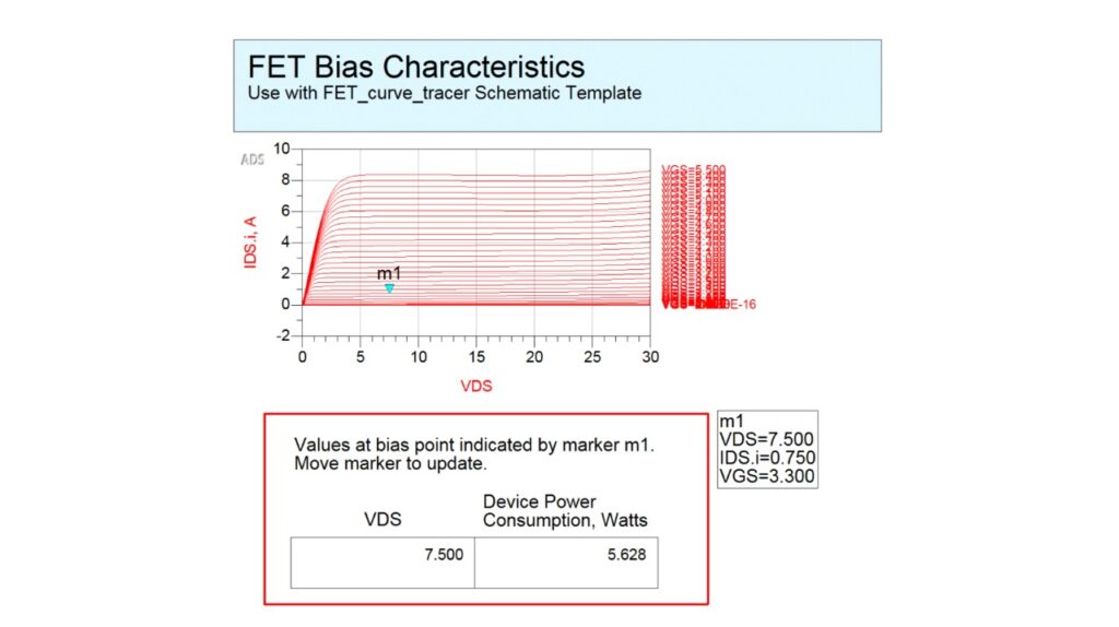
After resolving earlier indexing and equation issues in the DDS template, I reran the simulation and finalized all key parameter extractions. I placed the knee point marker at VDS ≈ 0.75 V, IDS ≈ 2.2 A, and the quiescent bias point at VDS = 7.5 V, VGS = 3.3 V, IDS = 0.75 A — values selected based on the curve tracer output and practical biasing considerations.

From the corrected DDS output, I obtained the following results:
| Parameter | Value |
| Load Resistance | 5.904 Ω |
| Max Output Power | 35.86 dBm |
| Small Signal Gain | 13.80 |
| Large Signal Gain | 12.32 |
| Voltage Swing (n_max) | 51.70 |
| DC Current (Idc) | 1 |
| Conduction Angle | 263.57 |
| Duty Cycle | 73.21 |
| Device Power (P_DC) | 5.862 |
These values confirm that the transistor is operating in Class AB mode with a wide conduction angle and high linearity potential suitable for my 161 MHz power amplifier design. With this solid baseline, I can now move on to stability analysis and eventually begin load-pull simulations to identify the optimal impedance environment for maximum output and efficiency. This final correction not only improved the accuracy of key metrics but also ensured that the DDS template runs reliably for future iterations.
Leave a Reply